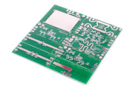
RF Circuit Board Design Challenges
RF Circuit Board Design
RF circuit boards are crucial to the operation of modern wireless communication and high-speed electronic devices. Their key challenge is to efficiently transmit and receive high-frequency signals. They must deal with many issues, such as noise and ringing caused by signal reflections. Moreover, they must be shielded from electromagnetic interference (EMI) from other components or external sources. They must also be able to minimize current loops, radiated emissions, and other problems that may cause a loss of signal integrity.
Fortunately, advanced PCB software and hardware help designers overcome these challenges. These tools offer various features that improve the performance of a printed circuit board, including simulation and optimization capabilities. This allows engineers to evaluate their design before prototyping and ensure that it meets the performance requirements of their system. They can also use simulation tools to optimize the placement of RF and non-RF components, ensuring that they work together without any interfering with each other.
One of the most important factors in rf circuit board design is impedance matching. This step is crucial to achieving an efficient transmission of a signal, and it involves adjusting the insertion losses, capacitance, and resistance of a PCB. It requires careful planning and analyzing to make sure that the resulting impedance matches the desired value. The best way to do this is by using a tool that can calculate the impedance of a circuit.

RF Circuit Board Design Challenges
Another key challenge is power routing, which involves maximizing the distribution of power across the PCB to ensure all active and passive components receive the necessary voltages and currents. In addition, proper routing helps prevent digital and analog noise from coupling to RF signals.
Proper grounding is also essential in RF PCBs. It is crucial to provide a continuous ground plane on the entire circuit, using conductive materials and via holes that are stitched together to prevent parasitic inductances. The grounding also reduces interference from other signal layers, minimizing EMI and maintaining signal integrity.
Character impedance is another critical factor in RF circuits, as it determines the ratio of voltages and currents that travel along a transmission line. It can be changed by the type of PCB material used, the thickness of the substrate, and other factors. To ensure that the resulting impedance matches the required value, designers should use a PCB that has a low dissipation factor and an appropriate dielectric constant.
To further enhance the quality of RF circuits, designers should consider using a Rogers laminate for the conductive layer and an inexpensive FR-4 for the remaining layers. This will allow them to save money on the cost of the PCB while achieving optimal performance. In addition, they should avoid using long stretches of parallel traces, as this will increase the coupling between them. Finally, they should use decoupling or bypass capacitors on each of the VCC and power supply lines to help them suppress noise at lower frequencies. This will help them maintain a higher signal quality at lower frequencies and eliminate flicker noise.