Assembly Techniques for Flexible PCB Boards
Techniques for Flexible PCB Boards
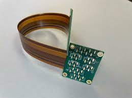
The flexible PCB, or flex PCB, is a type of printed circuit board that can be bent and twisted without affecting its performance. This type of PCB is used in various types of gadgets, from digital cameras and cell phones to robots and aerospace applications. The flexible PCB can be assembled using different assembly techniques, depending on its design and use.
As a result, it is important to understand the assembly process for flexible pcb board before purchasing them or commissioning them to be built. In this article, we will explore the flex PCB assembly process from start to finish, including all of the steps required to complete it successfully. We will also cover the benefits of a flexible PCB, as well as what to look for when choosing a provider to work with.
To begin, a flex PCB assembly must be designed with the utmost detail. This can be done with the help of CAD software programs and the assistance of experienced designers. The design should be made according to the specific needs of the project, including the number of layers and the thickness of the board. The design should also include details regarding the flexibility requirements of the flex circuit board.
Assembly Techniques for Flexible PCB Boards
The next step in a flex PCB assembly is preparing a bill of materials. This document lists all of the components that will be incorporated into the final product, as well as their individual part numbers and reference designators. Once the bill of materials is completed, it must be sent to a manufacturer for processing. Next, the bare board must undergo a process called baking, which is necessary to ensure that all of the humidity-sensitive materials are dry.
Once the bare boards are ready for assembly, they can be mounted with either surface-mount technology or through-hole technology. Surface-mount technology is typically used for smaller-in-size components, while through-hole technology is often utilized for larger and more complex devices. Once the components have been mounted, the flex PCB is then ready for re-flow soldering.
Routing traces on a flex PCB can be challenging, especially near bend areas. It is important to avoid crossing traces in these regions, and to stagger them rather than placing them adjacent to one another. This will prevent them from being damaged or ripped during the manufacturing and assembly processes.
In addition, it is vital to leave a sufficient amount of space between the drill hole and the copper. This will reduce the risk of the holes becoming damaged during the re-flow soldering process. It is also recommended to use a thicker solder paste when mounting components on flex PCBs, as this will increase the strength of the joints and help them stand up to any physical stresses that may occur during their use. Lastly, it is essential to use a high-quality solder paste that can withstand temperatures up to 250°C. With these tips in mind, you can be confident that your flex PCB will withstand the test of time.